- 您现在的位置:买卖IC网 > Sheet目录369 > W9751G6IB-25 (Winbond Electronics)IC DDR2-800 SDRAM 512MB 84-WBGA
�� �
�
�W9751G6IB�
�-1�
�0�
�1�
�2�
�3�
�4�
�5�
�6�
�7�
�8�
�9�
�10�
�11�
�12�
�CLK� /CLK�
�CMD�
�Active�
�A-Bank�
�Read�
�A-Bank�
�Write�
�A-Bank�
�WL=RL-1=4�
�AL=2�
�CL=3�
�DQS/DQS�
�≧� tRCD�
�RL=AL+CL=5�
�DQ�
�Dout0� Dout1� Dout2� Dout3�
�Din0�
�Din1�
�Din2�
�Din3�
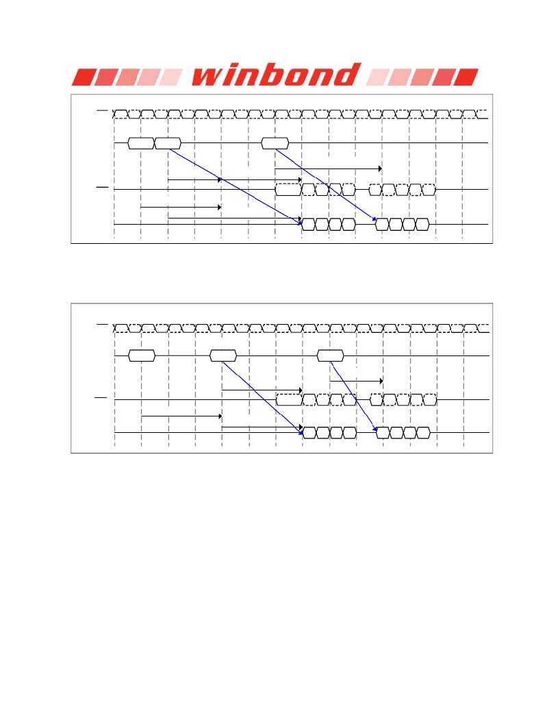
�[AL� =� 2� and� CL� =� 3,� RL� =� (AL� +� CL)� =� 5,� WL� =� (RL� -� 1)� =� 4,� BL� =� 4]�
�Figure� 14� —� Example� 1:� Read� followed� by� a� write� to� the� same� bank,�
�where� AL� =� 2� and� CL� =� 3,� RL� =� (AL� +� CL)� =� 5,� WL� =� (RL� -� 1)� =� 4,� BL� =� 4�
�-1�
�0�
�1�
�2�
�3�
�4�
�5�
�6�
�7�
�8�
�9�
�10�
�11�
�12�
�CLK/CLK�
�AL=0�
�CMD�
�Active�
�A-Bank�
�Read�
�A-Bank�
�Write�
�A-Bank�
�WL=RL-1=2�
�CL=3�
�DQS/DQS�
�≧� t� RCD�
�RL=AL+CL=3�
�DQ�
�Dout0� Dout1� Dout2� Dout3�
�Din0�
�Din1�
�Din2�
�Din3�
�AL� =� 0� and� CL� =� 3,� RL� =� (AL� +� CL)� =� 3,� WL� =� (RL� -� 1)� =� 2,� BL� =� 4]�
�Figure� 15� —� Example� 2:� Read� followed� by� a� write� to� the� same� bank,�
�where� AL� =� 0� and� CL� =� 3,� RL� =� (AL� +� CL)� =� 3,� WL� =� (RL� -� 1)� =� 2,� BL� =� 4�
�7.4.2�
�Burst� mode� operation�
�Burst� mode� operation� is� used� to� provide� a� constant� flow� of� data� to� memory� locations� (write� cycle),� or�
�from� memory� locations� (read� cycle).� The� parameters� that� define� how� the� burst� mode� will� operate� are�
�burst� sequence� and� burst� length.� The� DDR2� SDRAM� supports� 4� bit� and� 8� bit� burst� modes� only.� For� 8�
�bit� burst� mode,� full� interleave� address� ordering� is� supported,� however,� sequential� address� ordering� is�
�nibble� based� for� ease� of� implementation.� The� burst� length� is� programmable� and� defined� by� MR� A[2:0].�
�The� burst� type,� either� sequential� or� interleaved,� is� programmable� and� defined� by� MR� [A3].� Seamless�
�burst� read� or� write� operations� are� supported.�
�Unlike� DDR1� devices,� interruption� of� a� burst� read� or� writes� cycle� during� BL� =� 4� mode� operation� is�
�prohibited.� However� in� case� of� BL� =� 8� mode,� interruption� of� a� burst� read� or� write� operation� is� limited� to�
�two� cases,� reads� interrupted� by� a� read,� or� writes� interrupted� by� a� write.� (Example� timing� waveforms�
�refer� to� 10.13� and� 10.14� Burst� read� and� write� interrupt� timing� diagram� in� Chapter� 10)�
�Publication� Release� Date:� Oct.� 23,� 2009�
�-� 24� -�
�Revision� A06�
�发布紧急采购,3分钟左右您将得到回复。
相关PDF资料
W9751G6KB-25
IC DDR2 SDRAM 512MBIT 84WBGA
W9812G6JH-6I
IC SDRAM 128MBIT 54TSOPII
W9816G6IH-6I
IC SDRAM 16MBIT 50TSOPII
W9825G6JH-6I
IC SDRAM 256MBIT 54TSOPII
W9864G6JH-6I
IC SDRAM 64MBIT 54TSOPII
WM-5614
CABINET WALL MOUNT 37.25X17.9"
WRR-2244
RACK WALL MOUNT RELAY 42" X 19"
WRR-2264
RACK WALL MOUNT 75.25" X 19"
相关代理商/技术参数
W9751G6JB
制造商:WINBOND 制造商全称:Winbond 功能描述:8M ? 4 BANKS ? 16 BIT DDR2 SDRAM
W9751G6JB-25
制造商:Winbond Electronics Corp 功能描述:512GB DDRII
W9751G6JB-3
制造商:Winbond Electronics Corp 功能描述:512MB DDRII
W9751G6KB
制造商:WINBOND 制造商全称:Winbond 功能描述:8M ? 4 BANKS ? 16 BIT DDR2 SDRAM
W9751G6KB-18
制造商:Winbond Electronics Corp 功能描述:IC MEMORY
W9751G6KB-25
功能描述:IC DDR2 SDRAM 512MBIT 84WBGA RoHS:是 类别:集成电路 (IC) >> 存储器 系列:- 标准包装:1 系列:- 格式 - 存储器:闪存 存储器类型:闪存 - NAND 存储容量:4G(256M x 16) 速度:- 接口:并联 电源电压:2.7 V ~ 3.6 V 工作温度:0°C ~ 70°C 封装/外壳:48-TFSOP(0.724",18.40mm 宽) 供应商设备封装:48-TSOP I 包装:Digi-Reel® 其它名称:557-1461-6
W9751G6KB25A
制造商:WINBOND 制造商全称:Winbond 功能描述:Double Data Rate architecture: two data transfers per clock cycle
W9751G6KB25I
制造商:Winbond Electronics Corp 功能描述:DRAM Chip DDR2 SDRAM 512M-Bit 32Mx16 1.8V 84-Pin WBGA 制造商:Winbond Electronics Corp 功能描述:IC DDR2 SDRAM 512MBIT 2.5NS BGA